(晶圆)测试+清洁+修正,三合一黑科技(Ficontec+Femtum+Teradyne)精校字幕全文(中英文对照)

视频源自2025OFC,Louis Raff(CEO of femtum)的现场采访。原视频的AI字幕错误较多,无奈只能人工修正。附上精校字幕全文(中英文对照)。支持人提问没有收录,不影响理解。(晶圆)测试+清洁+修正,三合一设备由Ficontec+Femtum+Teradyne三家联合研制。Ficontec负责(硅光引擎)双面晶圆测试,运控,总装;Femtum提供3微米激光器;Teradyne提供电芯片测试器件。英伟达的20台订单总价据Patrick-jiucai估计4亿rmb左右,Ficontec占比本人估计50%以上(>2亿rmb)。而且这20台属于原型机,后面的追加订单值得期待。
视频链接:网页链接
up主把两段视频合在一起了,这篇的内容从3分10秒开始。
================================================================
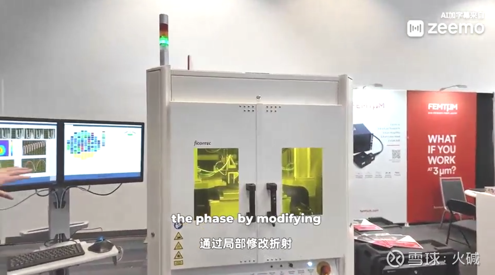
Louis Raff(CEO of femtum):This machine is the world’s first photonic wafer laser trimming in the world. Actually one of the biggest problem in the photonics is that the cost is still very high,and because the yield is very low. And what we doing here is basically changing the phase by modifying locally the refractive index with ultra-fast pulses, and we do this at wafer scale. We are indeed fixing broken chips on the wafer and it’s live right now. You have to do the first test and then when you know exactly the real response of the optical circuit,then you fix it with laser. It’s a bit like the LASIK for the eye,but for the waveguides. Exactly,and it’s a partnership with ficontec,so we’re adding optionality,and this can bring a lot of value to the customers.
这台设备是世界上首个用于光子器件的晶圆级激光修整系统。光子学领域目前最大的问题之一是成本仍然过高,因为良率非常低。我们在这里所做的,本质上是通过用超快激光脉冲局部修改折射率,从而改变相位,并且我们是在晶圆尺度上完成的。实际上我们就是在晶圆上修复坏掉的芯片,而且你看到的就是现场直播。你必须先做一次测试,然后知道光路的实际响应,再用激光进行修正。这有点像眼睛的激光矫正手术,但应用于波导。没错,这也是与Ficontec合作的成果,我们增加了可选性,这为客户带来了巨大的价值。
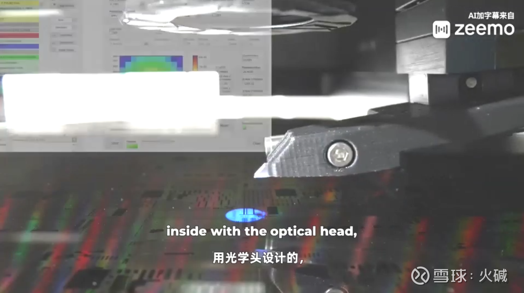
Louis Raff:this is a product,it’s a rack-mount fiber laser,everything has been designed inside with the optical head,it’s mass-manufacturable.
这是一款产品,是机架式光纤激光器,内部所有部分包括光学头都已完成设计,适合大规模量产。
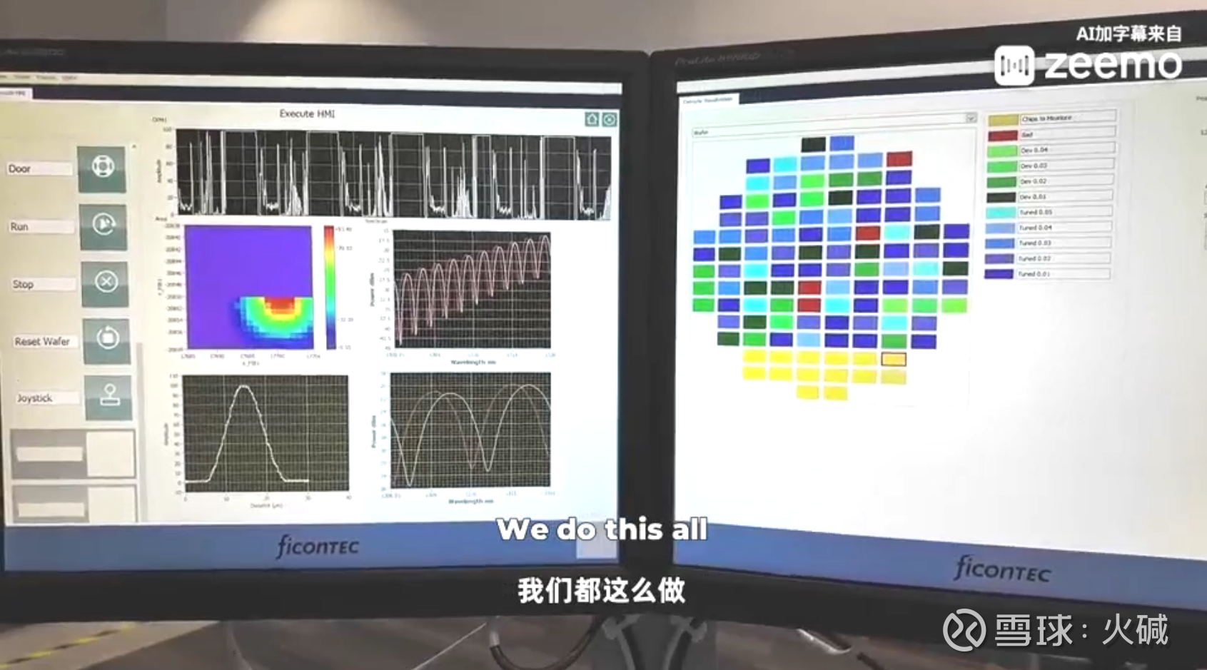
Louis Raff:What you’re looking at is the wafer map of the process variations.And here we are measuring is the first initial response of a Mach-Zehnder,it’s an unbalanced Mach-Zehnder which are used everywhere in the switches.They are used for filters,they are used for modulators and what we will see here in a few seconds,if you’re lucky we’ll see that the phase shift of an an unbalanced Mach-Zehnder is not spot on.What we have done here is predict the process parameters and correct the phase response and we can target and locate directly at 1310,which is a datacom wavelength.We do this all in an ultra-fast fashion.It’s quick,it’s permanent,it’s long-lasting.We have done a very nice reliability test,and it’s embedded now in the ficontec system.I’ll try just to open the door and stop the machine so you’ll be able to see the full thing. We have to wait a second it needs to finish one job and now it’s ok.So what you’re seeing here it’s a real wafer from a customer.It’s a six-inch wafer,you have a two-axis east-west optical probing,and you see the phantom head-inside it has collinear optics.We are focusing the beam right onto the waveguides and we are changing locally the refractive index. You have the vision,you have the illumination,you have the Galvo scanner,fiber beam delivery,everything is connected and ready to go.So that’s the beauty of the new photonic wafer laser trimming solution
你现在看到的是工艺变化的晶圆图。在这里我们测量的是马赫-曾德尔干涉仪的初始响应。这是一种非平衡马赫-曾德尔干涉仪,广泛应用于各类交换机中。它们可用于滤波器、调制器等。如果运气好,几秒钟后我们将看到非平衡马赫-曾德尔干涉仪的相移并非准确到位。我们在这里所做的就是预测工艺参数并校正相位响应,我们可以直接定位到1310nm(数据通信波长),我们以超快速的方式完成这一过程。它快速、永久且持久。我们进行了非常完善的可靠性测试,目前已集成到Ficontec系统中。我试着打开门,让机器停下来,这样你们可以看到整体情况。我们需要等一下,它得完成当前一个任务,现在好了。你现在看到的是客户提供的真实的晶圆。这是一片6英寸晶圆,正在进行东西方向的二维光学探针测试,你可以看到探针头里面是共线光学系统。我们正将激光束聚焦到波导上,并局部改变其折射率。这里具备视觉、照明、振镜扫描仪、光纤传输系统,所有设备都已连接完毕,随时可以工作。这就是全新光子晶圆激光修整解决方案的优势所在。
Louis Raff:So OFC2026, actually it will be a lot of first deployment with the customers.This project will come to a circuit level ,so we’re going to trim a lot of circuits,so a lot more data.
(展望明年)在OFC2026上,实际上我们会看到很多客户的首次部署。这个项目将应用到电路/光路层面,我们将修整大量电路/光路,从而获得更多的数据。
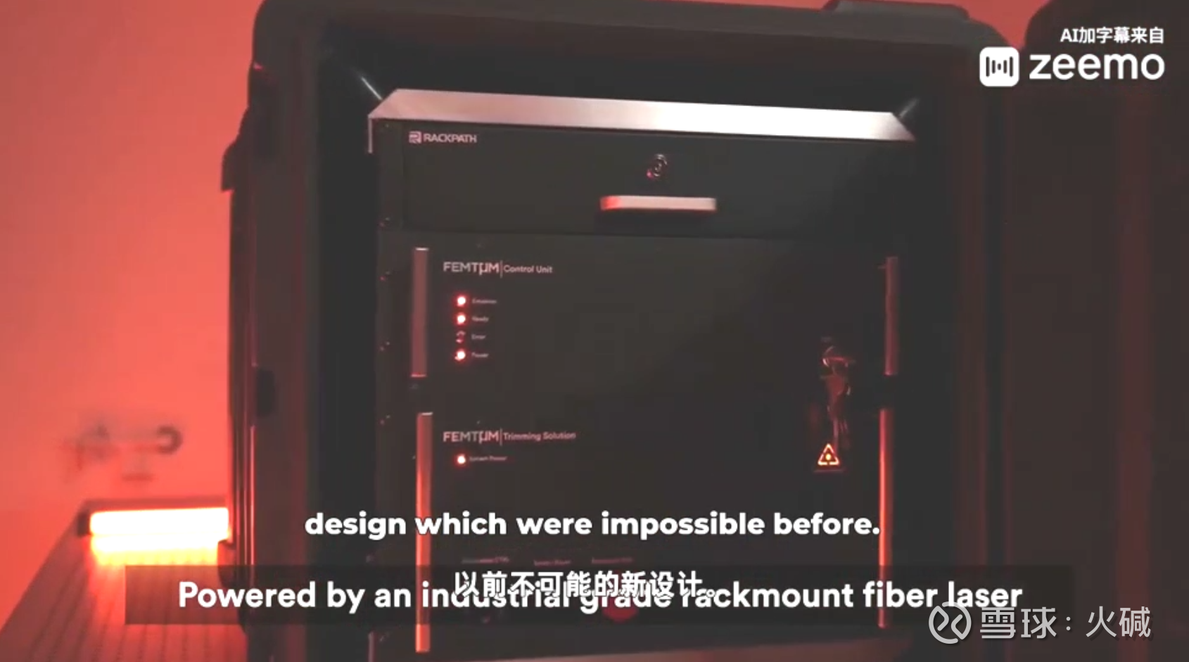
Louis Raff:So one of the critical things is that today designs of pics are very hard to the manufacture and the yields are low, and there’s a lot of impossible designs and with laser trimming with the post-fabrication reworking solution then you can extend the tolerances of the big design and actually deliver a new design which were impossible before.So the designers need to understand that now it’s possible to rework their photonic waveguides and basically make the yields higher
其中一个关键问题是,如今的光子芯片设计制造难度很大,良率低,设计上存在很多无法实现的环节。而通过激光修整这一后道可返工工艺解决方案,可以扩展大型设计的公差范围,实际上使以前不可能的设计成为可能。因此,设计师们需要认识到,现在可以对光子波导进行返工,从而大幅提高良品率。
Louis Raff:So 3-micron is key because you can be super selective to the right layer stack and you know semiconductors,we can use now multi-photon absorption process,and 3-micron enables that.So the laser source is really an enabler for the cleaning and the trimming.
3微米是关键,因为这能让你非常精确地选择目标堆叠层。在半导体领域,我们现在可以利用多光子吸收工艺,而3微米的波长使这一工艺成为可能。因此,激光源是实现清洁和修整的关键推动因素。
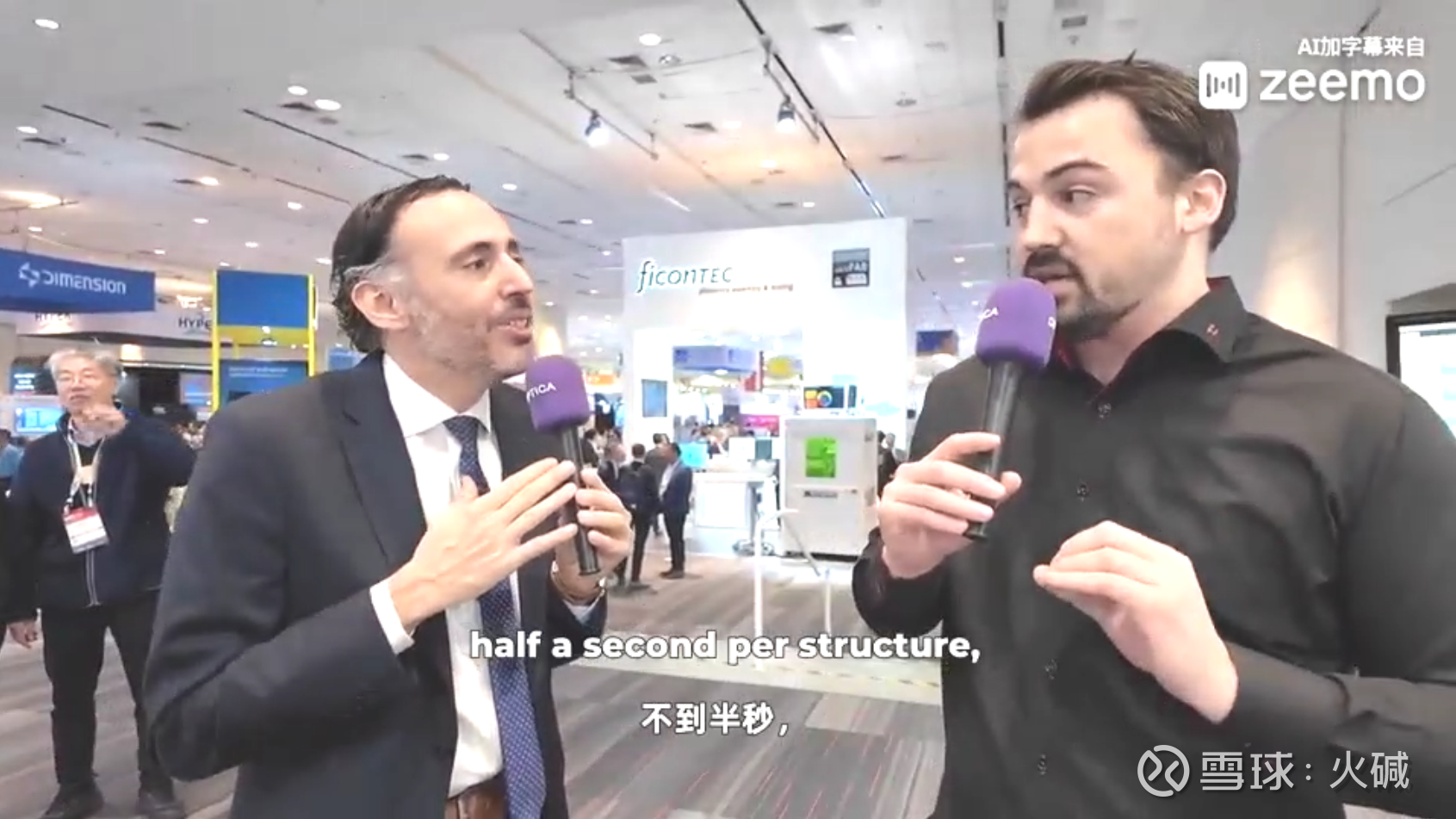
Louis Raff:The trimming actually is very fast and it’s at that speed.So it’s less than half second per structure,per circuit,it’s superfast with Galvo scanner.Actually what takes time is testing and motioning and people are pushing really hard with our partners to reduce that time.
修整过程实际上非常快,速度达到了每个结构、每个光路的处理时间不到半秒,这是利用振镜扫描仪实现的超快速处理。实际上耗时的部分是测试和运控,我们正与合作伙伴共同努力来减少这部分时间。
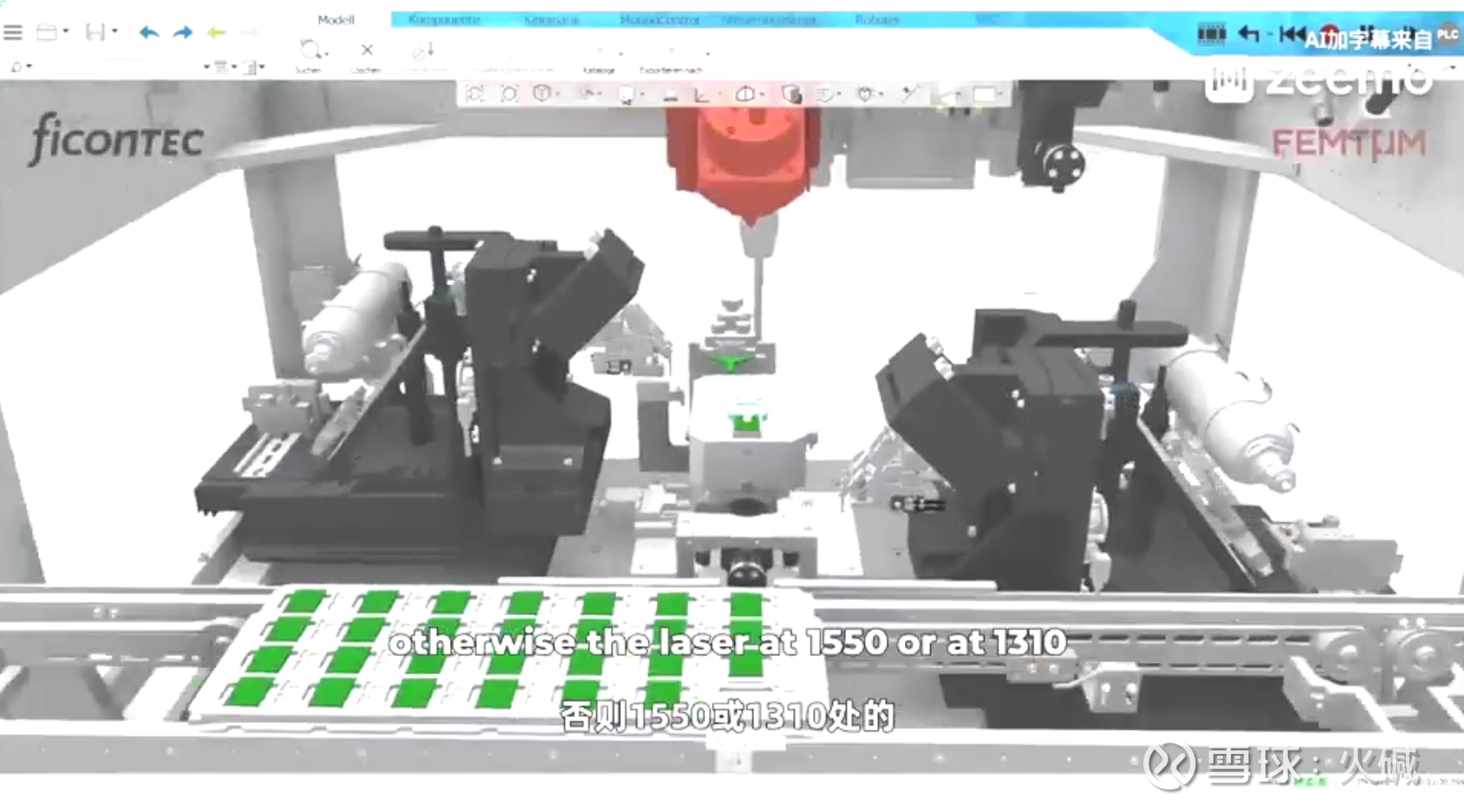
Louis Raff:2030 will be a crystal year for us because not only trimming will be everywhere,but cleaning as well.So a lot of advanced packaging right now requires a lot of clean surfaces and a lot of the cleaning are done manually.So what we do at femtum,we have developed an automated way to do the laser cleaning of photonic chips of CPO packages,of fibers,of the V-groove,and we make all those surface super clean so you can hit the yield that you want at scale.So if you can imagine,all those surfaces when you do the assembly,the bonding needs to be 100% cleaning because one particle will just do a misalignment and you will get optical losses,or it will be exactly at the coupling region and that coupling region needs to be 100% clean,otherwise the laser at 1550 or at 1310 will be hitting the particle and will burn.So it will be reliability issues.So actually,there’s a huge specs on getting everything clean and done quickly at the OSAT, at the back-end boundary line.So people right now everywhere are wiping off with Q-tips,and it’s done manually.It’s not automated and it’s known in the industry,all the OSATs are doing this like this right now.We shine pulses on the particle,the contaminant,and the residue.And since we have three micron laser technology,it’s selective and we can ablate the particle and the residue without affecting the substrate which are glass or silicon.
(展望2030年)2030年对我们来说将是一个突破性的一年,因为届时激光修整不仅会无处不在,清洁技术也将如此。目前许多先进封装都需要非常干净的表面,而许多清洁工作都是人工完成的。Femtum所做的,就是开发出一种自动化的方式,对光子芯片、CPO封装、光纤和V型槽进行激光清洁,使这些表面达到极致洁净,从而在量产中达到所需的成品率。你可以想象,当进行装配和键合时,所有表面都需要100%清洁,因为一个微小颗粒就会导致错位,产生光损耗,或者恰好出现在耦合区域。耦合区域必须完全洁净,否则1550nm或1310nm的激光会击中颗粒并将产生燃烧,从而导致可靠性问题。因此,在OSAT(外包半导体组装和测试)后端生产中,对快速高效清洁的要求非常高。目前行业内的普遍做法是用细棉签手动擦拭,所有OSAT厂商目前都还在采用这种方式。而我们Femtum则用3微米的激光脉冲照射颗粒、污染物和残留物,由于我们拥有3微米激光技术,具备选择性,可以在不影响基材(如玻璃或硅)的情况下清除污染物。
Louis Raff:So right now we are in very advanced process with key customers, I cannot say more about that,but we are at this stage,wear cleaning is also another big step forward for femtum.
目前我们正与关键客户进行非常深入的推进,但具体细节还不能透露。清洁领域也是Femtum迈出的另一大步。